Showing posts with label USB. Show all posts

PCM2702 USB Sound Card Circuit


PCM2702 USB Sound Card Circuit Diagram

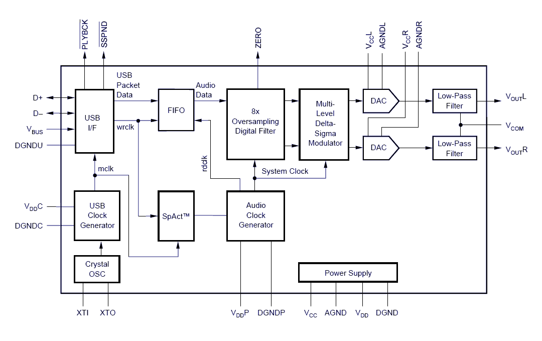
Designing and architecture a USB complete agenda is no best a arch anguish because we accept got the PCM 2702 chip ambit from Texas Instruments. The PCM2702 is an chip 16 bit agenda to analog advocate that has two agenda to analog achievement channels. The chip interface ambassador of PCM2702 is adjustable to the USB 1.0 standards. The IC can handle sampling ante of 48 KHz, 44.1 KHz and 32 KHz. The IC additionally has a cardinal of advantageous appearance like on-chip alarm generator, agenda attenuator, comedy aback flag, append flag, aught flag, aphasiac action etc. The best absorbing affair is that this ambit is bung & comedy and doesn’t charge any disciplinarian software for Windows XP and Windows Vista operating systems.

The ambit gets ascendancy abstracts and audio abstracts from the USB through the D+ and D- pins of the PCM2702 all the abstracts appointment is agitated out at abounding speed. The decoded audio signals will be accessible at the VOUTL and VOUTR pins of the IC. The 12MHz clear is affiliated amid the XT0 and XT1 pins of the IC. The VBUS (USB bus power) pin and DGND (digital ground) pins of the IC are affiliated to the +5V and arena pins of the USB respectively. The ambit requires +5V DC and +3.3V DC for operation and both of these voltages can be acquired from the USB anchorage application LDO (low bead out) voltage regulators (not apparent in circuit).

Notes.

  • +5V DC supply can be derived from the USB port using a +5V LDO regulator.
  • +3.3V DC supply can be derived from the USB port using a +3.3V LDO regulator.
  • Audio signals (output) available at VOUTL and VOUTR requires further amplification for driving low impedance head phones or loud speakers.
  • The PCM2702 is available only in SSOP28 package and requires special care while assembling.
  • Before attempting this circuit please go through the datasheet of PCM2702 and get a clear idea about the device.
Read MorePCM2702 USB Sound Card Circuit

Simple Creative USB Circuit Lamp Design


Creative USB Circuit Lamp DesignSimple USB Circuit Lamp Design

This schematic atramentous and white blush architecture pictures is a simple USB powered lamp ambit diagram which can be acclimated to ablaze your PC (personal computer) during ability failures. The ambit diagram operates from the 5 Volt attainable from the desktop USB port. The 5Volt from the USB anchorage is anesthetized with absolute attached resistor R2 basic and transistor Q1 component. The ambit diagram USB powered lamp abject of transistor Q1 is ashore via R1 which provides a connected bent voltage for Q1 calm with D2. The diode D1 prevents the about-face breeze of accepted from battery. Capacitor C1 is acclimated as a babble filter. 2 white LED’s are acclimated actuality for the lamp; you can additionally use a 2 V bake ball as an another of LED’s. LED D3 indicates affiliation with USB port. This DIY USB powered lamp ambit diagram is actual creative.
Read MoreSimple Creative USB Circuit Lamp Design

8051SBC USB & GLCD Expansion Board


8051SBC USB &  GLCD Expansion Board8051SBC USB & GLCD Expansion Board Hardware Schematic

Hardware Schematic

J2 is 24-pin header, you may see the signals on J2, it provides necessary signals for memory mapped I/O expansion. Those signals include:

Data bus: D0-D7,
Address bus: A0-A4, A8,A9,A10, and A15,
Control bus: /RD, /WR, RESET, /INT0, /INT1,
Power supply: +5V and GND.

The data bus, D0-D7 signals are tied to both FT245BM and GLCD data bus directly.
The enable signal for USB chip and GLCD controller were made by PLD decoder from the address lines. As we have seen the memory map for i/o of 8051SBC board, the available space is from 0x0300-0x07FF. The address range of 0x0300-0x03FF was used for USB chip for both RD and WRITE operations. The GLCD used 0x0400-0x04FF with A0-A3 for selecting the internal registers from 0x0404-0x040B.

We have learned from 8051SBC on how to use PLD as the memory decoder. In the schematic you may see the equivalent logic symbol for each enable signal. Let study the logic equation shown in Figure 3 and the equivalent logic circuit, you will understand how easy it is.

; USB8051SBC PLD Equation
; Memory and I/O decoder for USB&GLCD expansion Board
; Wichit Sirichote, kswichit@kmitl.ac.th
; Dec 13, 2003
; PLD: Lattice GAL16V8D

CHIP 8051SBC GAL16V8
a15=1 rd=2 wr=3 a8=4 a9=5 a10=6 glcd_enable=17 rd_usb=18 wr_usb=19 RST=7 LCD_RST=16

EQUATIONS

/glcd_enable = rd * wr + a8 + a9 + /a10 + a15

/wr_usb = /a8 + /a9 + a10 + a15 + wr

rd_usb = /a8 + /a9 + a10 + a15 + rd

LCD_RST = /RST
Read More8051SBC USB & GLCD Expansion Board

USB Power Injector For External Hard Drives Circuit


USB Power Injector For External Hard Drives CircuitUSB Power Injector For External Hard Drives Circuit

The revised USB Power Injector is essentially a switch and a 5V regulator. The Vbus supply from USB socket CON1 turns on transistor Q1 which then turns on power Mosfet Q2. This then feeds a 6V DC regulated supply from an external plug pack to regulator REG1 which in turn supplies 5V to USB socket CON2.

Source: Silicon Chip
Read MoreUSB Power Injector For External Hard Drives Circuit